
It might require a lot of training and patience to go from a mock-up version of a circuit board done on a breadboard, to designing your very own printed circuit board, or PCB for short. As you can imagine, there are various things that you need to learn about it, and this article might just help you with that.
Before taking a look at some other, important things, you should know that the PCB design takes place when the electric engineering procedure. It is what creates the “nervous system” and determines how a specific device works. Without it, you will be left with plastic and metal parts. Let’s take a look at the design and manufacturing processes of a PCB:
What You Should Know Before Starting The Design
The things you should determine before thinking about designing the PCB include:
- The Size – now, the size will mostly depend on the size of your product. The size of the item is also determined in the electric engineering procedure, hence, you can see why it is important.
- The Layers – adding more layers will require an intricate manufacturing process. Of course, even one layer is difficult to build. Not only will it be more complex to build, but it will also require more money. Two layers are usually used in simple items such as toys, four layers in IoT products, and six/eight layers are used for making smartphones or smartwatches.
- The Requirements a Manufacturer Needs – before the designing takes place, ensure that you know what the guidelines are for various things – including the isolation needed, the file naming, as well as the pacing. The information required includes how much layers you want it to have, the material, thickness, color, finish, the Gerber file, and the weight of the copper used.
What Does the Plan Include?
-
Designing the Circuit
The first you should do for this step is to create a chart. Now, this chart acts as a blueprint that describes how the parts connect with one another, as well as how they work. To produce this “blueprint”, you must use a program. There are various programs that you can use for creating one, and it will mostly depend on your preferences.
-
The Layout and The Gerber File
To make the layout and the Gerber file, again use the program specified in the step above. However, it can be a bit different. The layout should show the real sites of the parts featured on the PCB, and there should be a specific trace showing how the parts are connected between each layer.
Once you are done with designing the layout, you will be required to create a Gerber file. This is a file that the industrial company uses and there are thousands of businesses that can offer people these services. If you want to check out what service you can get, visit pcbonline.
-
The Fabrication
Once you send the Gerber file to the manufacturer you have chosen, they can start working on printing the board. This will be the starting point of building it even further, to adding the parts to the board and assembling the printed circuit board.
Preparing the Materials
By the time you reach this step, you should have selected all your components. You can opt for the manufacturer ordering all the parts needs, or you can do it bu yourself by ordering them from the vendors you want. Some things that you should remember include:
- The Time Needed for the Part to Arrive – since you or the manufacturing company will order the parts from different vendors, you should know that it will take some time for them to arrive. You might need to wait for about 7 to 15 weeks for some parts to arrive.
- The Package – consider ordering the parts in reels, not in different packages.
- Inquire About the MOQ – always remember to inquire about the minimum order quantity of the parts. If the quantity is smaller order them from online vendors, but if it is a bigger quantity, ask the manufacturer for some recommendations.
- Consider the Losses – if you want to be prepared for some losses, order at least 10 percent more – of course, it would be crazy if you placed an additional 10 percent order for the high-priced parts, hence, this tip only applies to the cheaper ones.
The Assembly
There are two mounting techniques to choose from:
- A Thru-hole – which is a manual technique for putting the parts on the board with wire leads. The wire leads are, as the name implies, placed through the openings on the exterior area. It is also referred to as the Dual In-line Package method.
- A Surface Mount Tech – is the one that is commonly used. This method incorporates machines, hence, they will accurately assemble it, which in return means more time- and money-efficiency for you.
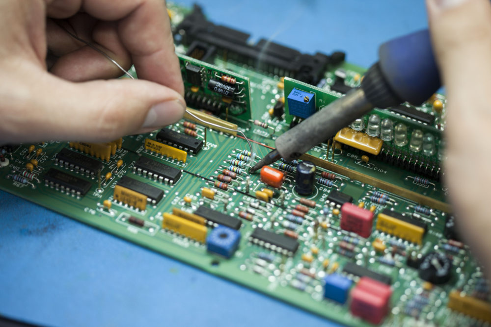
What Soldering Techniques to Opt For?
The most common technique utilized is a reflow one, and it is what makes all parts stay on the PCB. It either goes through an infrared light or a furnace that burns the board until the solder melts. This is how the parts stay on it permanently.
For this step, it is extremely crucial that you picked a manufacturer that is well-respected since no parts should be damaged or overheated. Some other techniques include the wave soldering which requires the parts to be installed manually, and iron soldering which can be implemented in particular situations, however, it is not usually practiced in large production plants.
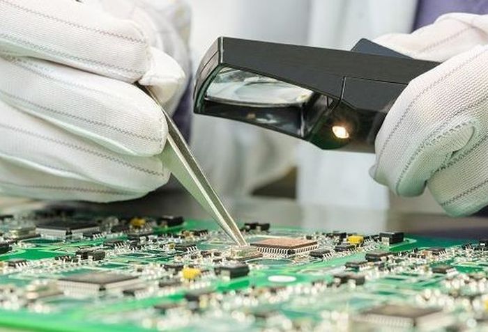
Testings the Board
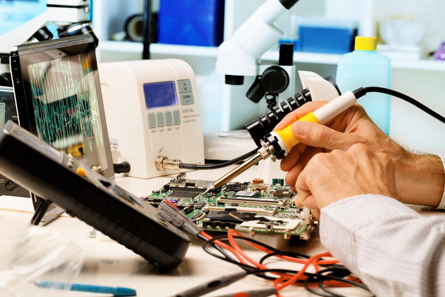
During this step, you will need to test a sample of the printed circuit boards in order to verify the quality. Some of the most common problems that can be found are the parts not being properly attached, parts being misaligned, and shorts that are connected to different parts of the board which should not be connected at all. The tests that you should perform include the ICT test, AOI, and an X-ray.
Conclusion
As you can see, designing and manufacturing a printed circuit board is a process that is incredibly complex and difficult. Hence, now that you know what you need to consider and do, do not waste any more time and start creating a plan for designing a printed circuit board.


